國立台灣大學林清富教授實驗室
研究領域摘要
主題八: 矽微米球共振腔
研究人員: 許書嘉 、 洪士哲
英文摘要:
Microspheres support ultra-low-loss whispering-gallery modes (WGMs) when evanescently excited from adjacent waveguiding structures. The high quality
factor (Q) and small mode volume associated with WGMs makes the microspheres suitable for numerous optical devices, such as microlasers, narrow optical
filters, optical switching, ultrafine sensing, displacement measurement, rotation detection, high-resolution spectroscopy, and Raman sources. However, most of
the research with spherical structures is based on noncrystalline materials such as glass or polymers. Little literature reported microspheres on crystalline
materials, like semiconductor, in the past.
Since silicon is the dominating material in current integrated circuit industry, fabricating microspheres on a Si-based substrate contributes to compact and low-
cost photonics for mass-market applications. Here, we present a technique applying the homogenized KrF excimer laser reformation to fabricate Si spheres on
the SOI platform. It is capable of fabricating Si spheres with extremely smooth surface. AFM measurement shows that the root-mean-square roughness (RMS-
roughness) of the surface of the fabricated sphere is smaller than 0.1 nm. In addition, the selective exposure of excimer laser makes the high power laser only
work on the desired region. This outstanding property makes the process compatible with modern ULSI electronics. Furthermore, single-crystalline was
amazingly observed after total transformation of the Si profile from a rod into a sphere. In this paper, we describe the laser reformation technique and the
fabrication process in detail. The fabricated results are examined by scanning electron microscopy (SEM), atomic force microscopy (AFM) and tunneling
electron microscopy (TEM).
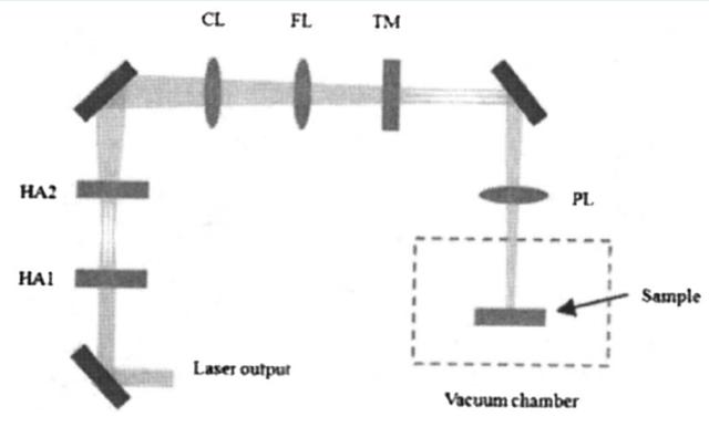
Fig.1 The diagram of homogenized KrF excimer laser reformation system.
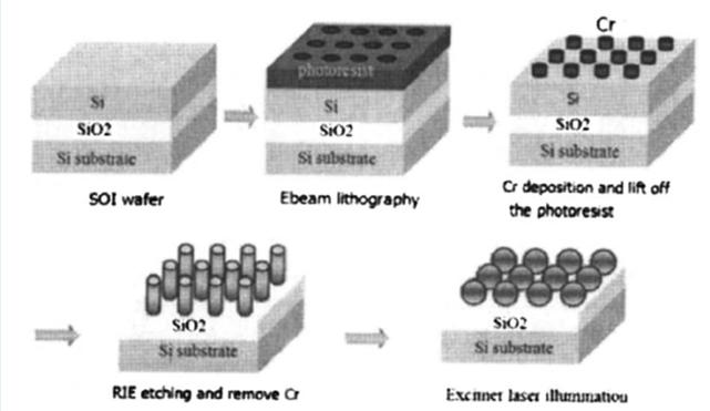
Fig.2 The flow chart of fabrication process.
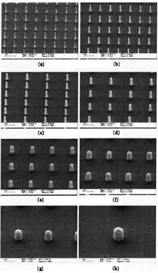
Figs.3 The 30 degree-tilted SEM images of the samples after RIE etching.
The diameters of the Si rods are (a) 40 nm, (b) 85 nm, (c) 170nm, (d) 210 nm, (e) 320 nm,
(f) 450 nm, (g) 660 nm, and (h) 940 nm.
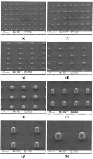
Figs.4 The SEM images of Si structures after excimer laser reformation.
Figs. 4 (a)-(h) are corresponding structures to Figs. 3.
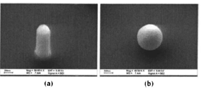
Figs.5 50000x, 30 degree tilted SEM images in the spherical case. (a) Before illumination (b) After illumination.
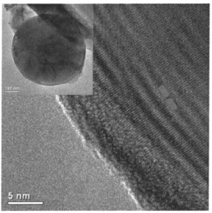
Fig.6 TEM image of the fabricated Si sphere. The insert figure is the TEM profile of the detected sphere.
中文摘要:
微米球能夠達到超低光損耗的迴廊共振模態,其擁有超高的品質因子(Q-factor)以及很小的模態體積,這使得微米球可以被應用於很多的光學元
件,其中包括了微米雷射(microlasers)、窄頻寬光濾波器(narrow optical filters)、光子開關(optical switching)、超細微靈敏感測器(ultrafine sensing)、
位移偵測(displacement measurement)、rotation detection、高解析頻譜(high-resolution spectroscopy)和拉曼源(Raman sources)。然而,大多數研究製作
微米球結構都採用非晶材料,例如玻璃或高分子材料,只有很少數的文獻報導使用晶體材料製作微米球,例如半導體材料。
因為矽材料是目前積體電路主要的材料,製作矽微米球於矽基板上將可以整合於低成本的矽基電路當中。這裡,我們展示了利用準分子雷射退
火重新塑造矽微米結構成矽微米球。原子利顯微鏡的測量發現微米球的表面粗糙度低至0.1奈米,此外。準分子雷射擁有選擇照射特定區域的功
能,可以只照射在所需得區域,這個優點未來將可以整合於積體電路的製程當中。更進一步地,我們發現矽微米球有很好的結晶特性,利用穿
透式電子顯微鏡發現其結構為單晶結構。